Konferenzen > Physik > Halbleiterphysik
Wählen Sie ein Land aus
ALLE LÄNDER (10)
1
International Conference on Compound Semiconductor Manufacturing Technology
20. Mai 2024 - 23. Mai 2024 • Tucson, AZ, Vereinigte Staaten
2
DSQT 2024 — Defects in solids for quantum technologies
10. Jun 2024 - 14. Jun 2024 • Budapest, Ungarn
Eintrags-ID:
1592419
Webseite:
3
816. WE-Heraeus-Seminar — Silicon Carbide: Classical and Quantum Technologies
28. Jul 2024 - 31. Jul 2024 • Physikzentrum Bad Honnef, Deutschland
Eintrags-ID:
1602121
4
Optica Advanced Photonics Congress — Integrated Photonics Research, Silicon and Nanophotonics (IPR) .
28. Jul 2024 - 01. Aug 2024 • Québec City, Québec, Kanada
Eintrags-ID:
1581860
5
Optica Advanced Photonics Congress — Solar Energy and Light Emitting Devices (SOLED) .
28. Jul 2024 - 01. Aug 2024 • Québec City, Québec, Kanada
Eintrags-ID:
1581921
6
ICPS 2024 — International Conference on the Physics of Semiconductors
28. Jul 2024 - 02. Aug 2024 • Ottawa, Ontario, Kanada
Einsendeschluss für Abstracts:
01. Apr 2024
Eintrags-ID:
1592656
7
ESD, EOS — 46TH ANNUAL EOS/ESD SYMPOSIUM & EXHIBITS
09. Sep 2024 - 19. Sep 2024 • Reno, Vereinigte Staaten
Eintrags-ID:
1612699
8
SPIE Photomask Technology + Extreme Ultraviolet Lithography
29. Sep 2024 - 04. Okt 2024 • Monterey, Kalifornien, Vereinigte Staaten
Eintrags-ID:
1592847
9
BCICTS — 2024 IEEE BiCMOS and Compound Semiconductor Integrated Circuits and Technology Symposium
13. Okt 2024 - 16. Okt 2024 • Fort Lauderdale, FL, Vereinigte Staaten
10
821. WE-Heraeus-Seminar — Uniting Today’s Nanotechnology for Advancing Tomorrow’s Semiconductor Physics
13. Nov 2024 - 15. Nov 2024 • Physikzentrum Bad Honnef, Deutschland
Conference-Service.com stellt der Öffentlichkeit ein Kalendarium wichtiger Konferenzen, Symposien und sonstiger Tagungen im wissenschaftlich-technischen Bereich zur Verfügung. Obwohl das Verzeichnis mit großer Sorgfalt zusammengestellt und ständig aktualisiert wird, weisen wir auf die Möglichkeit von Fehlern ausdrücklich hin. Bitte vergewissern Sie sich immer beim Veranstalter, bevor Sie über die Teilnahme oder Nichtteilnahme an einer Konferenz entscheiden.

Kein Tracking | Keine Pop-ups | Keine Animationen
Stand vom 26. März 2024
Konferenzkalender nach Gegenstand
-
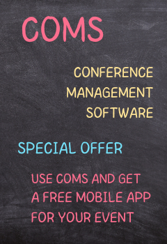
 COMS benutzen und entspannen!